Home
» Technology
»
Where Should You Study Semiconductor Engineering? 8 Chip Design Schools to Compare in 2026
Where Should You Study Semiconductor Engineering? 8 Chip Design Schools to Compare in 2026
Choosing where to study semiconductor engineering is really a choice about which part of the chip stack you want to learn deeply. A student who wants to design mixed-signal integrated circuits needs a different environment from someone who wants to develop transistor materials, run process steps in a cleanroom, or optimize semiconductor manufacturing. That is why a useful school comparison should focus on verifiable program strengths instead of declaring one university the best for everyone.
This guide compares eight U.S. universities using current official program and research information available in September 2026. The list is not a numerical ranking. It is a practical shortlist built around chip design, semiconductor devices, fabrication, research infrastructure, and degree pathways.
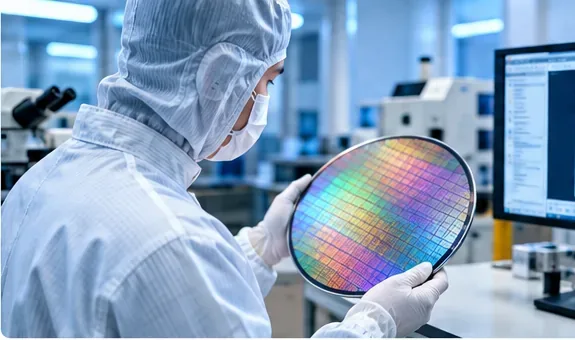
A cleanroom researcher examines a patterned silicon wafer, representing the fabrication and device side of semiconductor engineering that complements IC and chip design.
What do you actually want to study: chip design, semiconductor devices, or manufacturing?
Before comparing schools, separate several fields that are often grouped under the phrase “semiconductor engineering.” They overlap, but the coursework and laboratory experience can be quite different.
Integrated circuit and VLSI design: digital, analog, mixed-signal, RF, power, memory, system-on-chip design, verification, physical design, and electronic design automation.
Semiconductor devices and materials: transistor physics, compound semiconductors, photonics, emerging materials, device modeling, and characterization.
Fabrication and process technology: lithography, deposition, etching, implantation, process integration, cleanroom work, and manufacturing.
Packaging, test, and reliability: chiplets, interconnects, advanced packaging, test methodology, yield, thermal issues, and reliability.
Computer architecture and hardware systems: accelerators, memory systems, domain-specific hardware, and hardware-software co-design.
If your goal is to become an IC designer, prioritize schools with active circuit groups, modern EDA workflows, and evidence of prototype-chip work. If you want a fabrication or process career, cleanroom access, device courses, and process-integration work matter more. If you are not yet sure, a broad semiconductor program may be safer than a narrow circuit-only track.
What should you compare before choosing a semiconductor school?
Criterion
What to verify
Main tradeoff
IC design depth
Analog, digital, mixed-signal, RF, VLSI, CAD/EDA, verification, and physical-design courses or research groups
A strong design school may offer less fabrication exposure
Prototype and tape-out culture
Research groups that fabricate or measure ASICs, CMOS prototypes, or silicon test chips
Most tape-out access is concentrated in advanced courses and graduate research
Device and fabrication infrastructure
Nanofabrication, process, materials, and characterization facilities
Device-heavy programs may be less focused on full-chip architecture or RTL-to-layout workflows
Degree structure
Dedicated semiconductor major, concentration, certificate, ECE track, or research specialization
A dedicated label is convenient, but a broader EE/ECE degree can offer more flexibility
Faculty and lab fit
Several faculty working in the exact area you want, not just one professor
Faculty availability and funded projects can change from year to year
Industry access
Industry-sponsored centers, internships, professional programs, and regional semiconductor activity
Strong local industry access can come with higher living costs or a more competitive internship market
Do not rely on a single course title or a university-wide ranking. Read the actual lab pages, course catalog, and degree requirements. Also check whether undergraduates can join the relevant labs, because some advanced chip-design and fabrication opportunities are primarily graduate-level.
Which schools are strongest for different semiconductor goals?
MIT: best fit for research that connects devices, circuits, and new technologies
MIT is especially compelling if you want research that spans from materials and nanoscale devices to integrated circuits and systems. The Microsystems Technology Laboratories describes work across integrated circuits, electronic and photonic devices, MEMS, nanoscale technologies, sensors, and emerging architectures, with shared nanofabrication and characterization infrastructure. MIT EECS also maintains a dedicated integrated-circuits-and-systems research area.
Choose MIT if: you want a research-intensive path, expect to continue into graduate study, or want to work across the boundary between device technology and circuit/system design.
Tradeoff: MIT is not simply a “semiconductor engineering major” experience. Students often build a semiconductor focus through EECS coursework and research, so you need to plan your path deliberately.
Stanford: best fit for application-driven IC design and advanced circuit research
Stanford Electrical Engineering lists integrated circuits and systems as an active research area covering mixed-signal ICs, RF and millimeter-wave ICs, power electronics, nanosystems, and silicon technology modeling. That breadth makes Stanford particularly attractive to students who know they want circuit design but have not yet decided between analog, RF, mixed-signal, power, or emerging-device-enabled systems.
Choose Stanford if: your priority is graduate-level IC design research, especially mixed-signal, RF/mm-wave, power, or hardware built around advanced device technologies.
Tradeoff: the program is broad EE rather than a narrowly packaged semiconductor degree. Students who want process manufacturing as the dominant focus should verify that their intended lab and coursework provide enough fabrication exposure.
UC Berkeley: best fit for prototype chips, mixed-signal design, and design methodology
Berkeley’s Wireless Research Center is unusually explicit about prototype-chip work. Its research spans analog, digital, mixed-signal, RF, wireline, chiplet-design tools, design automation, AI accelerators, and other integrated systems. The center states that ASIC proof-of-concept chips are fabricated using advanced process technologies and evaluated in an in-house laboratory.
Choose Berkeley if: you want a strong circuit-design ecosystem with a visible path from architecture and circuit ideas to fabricated prototypes and measurement.
Tradeoff: BWRC is research-centered, so the richest tape-out experience may be concentrated in graduate research rather than guaranteed to every undergraduate.
Purdue: best fit for a broad, explicitly semiconductor-focused degree ecosystem
Purdue stands out because its Semiconductor Degrees Program is structured around the semiconductor field itself rather than asking students to assemble a specialization informally. Purdue lists more than 100 semiconductor-related courses spanning chip design, manufacturing, advanced packaging, materials, equipment, and supply-chain topics. It offers undergraduate certificates, concentrations and a minor, graduate concentrations, and an online interdisciplinary master’s in microelectronics and semiconductors.
Choose Purdue if: you want a clear semiconductor credential, want flexibility across design and manufacturing, or are a working professional seeking an online graduate route.
Tradeoff: the breadth is a strength, but students focused specifically on front-end IC design still need to select design-heavy courses and labs rather than assuming every semiconductor pathway is circuit-centric.
UT Austin: best fit for a focused graduate track in integrated circuits and systems
UT Austin offers a formal Integrated Circuits and Systems graduate track covering digital, analog, mixed-signal, and RF ICs, along with verification, testing, CAD, high-performance and low-power design, and design for manufacturability. The university’s Integrated Circuits and Systems Group also brings together multiple faculty working across those areas.
Choose UT Austin if: you already know you want IC design and want a graduate curriculum organized directly around circuits, implementation, verification, and CAD.
Tradeoff: students more interested in semiconductor process technology than in circuit design should also investigate the Microelectronics Research Center and device-oriented courses rather than relying only on the ICS track.
University of Illinois Urbana-Champaign: best fit for students who want both circuits and device physics
Illinois ECE separates but strongly supports both circuits and microelectronics. Its circuits research includes low-power nanoscale ICs, system-on-chip design, mixed-signal ICs, CAD, physical design, reliability, and design for manufacturing. Its microelectronics and photonics work adds semiconductor materials, device physics, silicon photonics, III-V devices, terahertz devices, and other emerging technologies.
Choose Illinois if: you want room to move between chip design, CAD, device modeling, and semiconductor-device research without leaving the same ECE ecosystem.
Tradeoff: because the department is broad, you must identify your intended faculty group and course sequence instead of expecting one unified semiconductor curriculum.
Georgia Tech: best fit for students who want design, fabrication, and test in one engineering environment
Georgia Tech’s Electronic Design and Applications area explicitly connects device and integrated-circuit fabrication with circuit and system design, simulation, instrumentation, and testing. Its Integrated Circuits and Systems Research Lab describes silicon design, tape-outs, measurements, scaled CMOS work, on-chip sensors, mixed-signal circuits, machine-learning hardware, memories, and power-management circuits.
Choose Georgia Tech if: you want to understand the full path from devices and fabrication through circuit implementation and measured silicon.
Tradeoff: as with MIT, Stanford, Berkeley, and Illinois, semiconductor study is embedded inside a broad ECE structure rather than packaged as one simple undergraduate “semiconductor engineering” major.
Arizona State University: best fit for an undergraduate who wants an explicit microelectronics curriculum
ASU offers a Bachelor of Science in Engineering Science with a Microelectronics concentration. The official program description says students build foundations in math, coding, digital design, and physics, then learn tools used to design and fabricate microelectronic circuits, followed by final-year work in semiconductor testing, development, and manufacturing plus a year-long capstone.
Choose ASU if: you want a clearly named undergraduate microelectronics path that combines design, fabrication, testing, and manufacturing rather than waiting until graduate school to specialize.
Tradeoff: the program is a concentration within Engineering Science, so applicants should inspect the current major map, campus location, electives, and lab opportunities to ensure the balance matches a chip-design versus manufacturing goal.
Verify current campus, electives, and advanced design depth
Should an undergraduate choose a semiconductor-specific major?
Not necessarily. A dedicated semiconductor or microelectronics label can make course planning easier, especially if you already know you want fabrication, manufacturing, test, or packaging. Purdue and ASU are attractive for that reason. But many elite chip designers still begin with a broad electrical or computer engineering degree and specialize through VLSI, analog IC, RF IC, device physics, CAD, or research projects.
For an undergraduate, a broad ECE degree can also reduce risk. If you later discover that you prefer computer architecture, embedded systems, signal processing, or software, you retain more room to pivot. The key is not the degree title; it is whether you can build the right sequence of courses and projects before graduation.
Is tape-out experience more important than a famous school name?
For design-focused roles, a serious chip project can be extremely valuable because it forces you to work through constraints that classroom problem sets may not expose: verification, timing, layout, parasitics, interfaces, measurement planning, and the reality that a fabricated design cannot be patched like ordinary software. However, not every student at a famous semiconductor school will automatically tape out a chip.
When evaluating programs, ask whether students in your degree level can participate in ASIC or mixed-signal prototype projects, what EDA tools are used, whether fabrication runs are part of courses or research, and whether you will be able to measure silicon after fabrication. Berkeley and Georgia Tech publish particularly clear evidence of fabricated prototype and tape-out activity, while other schools may offer similar opportunities through individual labs.
What should you ask before applying?
Can students at my degree level take advanced VLSI, analog IC, RF IC, digital IC, physical-design, semiconductor-device, or process-integration courses?
Which faculty are actively accepting students in the area I want?
Can undergraduates join those labs, or is participation mainly for MS and PhD students?
Are there recent examples of fabricated chips, measured silicon, cleanroom projects, or semiconductor capstones?
Does the curriculum use contemporary EDA flows, and are tool licenses available for student projects?
If I want manufacturing, packaging, or process engineering, are those subjects central or merely optional electives?
What are the actual tuition, fees, assistantship rules, and living costs for the year I plan to enroll?
That last question deserves special attention. This article intentionally does not compare tuition because published costs, residency rules, financial aid, and graduate funding change frequently and can differ sharply by degree level. Check each university’s current admissions and financial-aid pages before making a cost decision.
Which school should you choose?
If your goal is deep IC design research, Stanford, Berkeley, and UT Austin deserve close attention. If you want to work across devices, nanofabrication, and circuits, MIT, Illinois, and Georgia Tech offer strong multidisciplinary environments. If you want an explicit semiconductor-focused educational path, Purdue is unusually broad across degree levels, while ASU offers a clearly defined undergraduate microelectronics concentration.
The strongest choice is the school where the curriculum, faculty, labs, and project access all line up with the kind of semiconductor engineer you want to become. Start with the field you want to practice, identify three to five faculty or labs that genuinely match it, and then compare degree structure, project access, cost, and location. That approach is more useful than choosing a university from a generic ranking and hoping the specialization appears later.