Home
» Technology
»
Inside the Global Race for Advanced Chip Packaging and Fabrication
Inside the Global Race for Advanced Chip Packaging and Fabrication
A practical problem is becoming harder to ignore across the semiconductor industry: building a leading-edge chip is no longer just about printing smaller transistors. A cutting-edge AI accelerator can still miss its performance, cost, or delivery targets if high-bandwidth memory cannot be placed close enough to the logic, if an interposer is too large or expensive, if package yield is poor, or if advanced assembly capacity is located far from the wafer fab.
That is why the global semiconductor race in 2026 is increasingly a race across two connected fronts. The first is fabrication: gate-all-around transistors, backside power delivery, EUV lithography, yield, and capacity at roughly the 2nm class and beyond. The second is advanced packaging: chiplets, 2.5D interposers, 3D stacking, hybrid bonding, high-bandwidth memory integration, substrates, testing, and thermal management.
The distinction matters because a country or company can be strong in one layer and still depend heavily on another region for the rest of the system. For customers buying AI infrastructure, for governments funding semiconductor programs, and for companies planning supply chains, the key question is no longer simply “Who has the smallest node?” It is “Who can manufacture, integrate, test, and scale the entire system?”
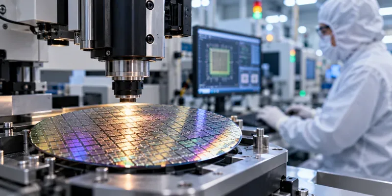
A semiconductor wafer under precision inspection equipment illustrates the front-end manufacturing side of a race that increasingly depends on advanced packaging and system integration as well.
Why packaging has become a first-order performance constraint
For decades, semiconductor progress was commonly summarized by transistor scaling. That remains important, but modern AI and high-performance computing systems are pushing against other physical limits at the same time.
One limit is die size. Lithography tools expose a finite field, so designers cannot simply make a monolithic processor arbitrarily large. Chiplets offer another path: divide a system into smaller dies and connect them with very high-bandwidth links inside one package. A second limit is memory bandwidth. AI accelerators need enormous data movement between logic and high-bandwidth memory (HBM), so distance, routing density, power delivery, and package geometry matter directly to system performance.
A third limit is economics. Very large leading-edge dies can be expensive because a defect can ruin a large amount of valuable silicon. Chiplet architectures can let designers put only the functions that truly need an advanced process on the most expensive node while using older or specialized nodes for I/O, analog, cache, or other functions. The trade-off is that packaging becomes much more difficult.
That is why terms such as CoWoS, SoIC, EMIB, Foveros, I-Cube, X-Cube, hybrid bonding, redistribution layers, and silicon bridges now appear in discussions that once focused almost entirely on process nodes.
The fabrication race: 2nm-class production is becoming real
TSMC: scaling N2 while pushing backside power and larger systems
TSMC states that its N2 process entered high-volume manufacturing in the fourth quarter of 2025 with good yield, and that N2P and A16 were scheduled for volume production in the second half of 2026. A16 adds TSMC’s Super Power Rail backside power technology for designs with demanding power-delivery and routing requirements. See TSMC’s 2025 annual report and its A16 technology overview.
The important point is not the marketing label attached to a node. Node names are not literal transistor dimensions and are not directly comparable across foundries. What matters is whether a process reaches acceptable yield, performance, power, density, design-tool maturity, and production volume for real customer products.
Intel: 18A combines gate-all-around with backside power
Intel says Intel 18A entered production in 2025 and is now in high-volume production in the United States. The process combines RibbonFET gate-all-around transistors with PowerVia backside power delivery. Intel also reported in June 2026 that the enhanced 18A-P variant had entered risk production. The company’s current material on Intel 18A distinguishes production status from future variants and provides the process claims with supporting technical references.
Intel’s strategy is particularly notable because it pairs front-end manufacturing with a large domestic advanced-packaging footprint. That matters for customers that want process technology, assembly, testing, and supply-chain geography to be planned as one system rather than as separate purchases.
Samsung: 2nm expansion tied to memory and packaging
Samsung’s foundry roadmap uses gate-all-around technology and increasingly ties its logic offerings to the company’s memory and advanced-package businesses. In its second-quarter 2026 results, Samsung said it planned to ramp production of new mobile products on its second-generation 2nm process during the second half of 2026 and reported expanding 2nm HPC engagements. Separately, Samsung and Broadcom announced a 2026 collaboration spanning 2nm-and-below foundry technology, HBM, and advanced packaging. See Samsung’s Q2 2026 results and the Samsung-Broadcom announcement.
The strategic advantage Samsung is trying to create is obvious: logic, memory, and packaging can be co-optimized. The challenge is equally clear—customers still judge a foundry by production yield, schedule reliability, ecosystem readiness, and the competitiveness of the final packaged system, not by a roadmap slide alone.
Japan’s Rapidus: a bid to re-enter leading-edge logic
Rapidus is attempting something different: rebuilding a leading-edge logic manufacturing base in Japan around a 2nm gate-all-around process. Its IIM-1 pilot line in Chitose began operating in April 2025, and Rapidus says mass production is targeted for 2027. In April 2026, Japan’s NEDO approved Rapidus’ fiscal-year plan covering both 2nm front-end development and chiplet/package design and manufacturing. Rapidus also reported a 600mm-square organic RDL interposer prototype and plans to verify 2.xD and 3D package processes at its Rapidus Chiplet Solutions facility. See Rapidus’ FY2026 project update.
This remains a forward-looking manufacturing program rather than proof of 2027 mass-production success. That distinction is important: prototype transistors, a working pilot line, a usable PDK, customer tape-outs, production yield, and sustainable high-volume manufacturing are separate milestones.
The packaging race: the package is becoming part of the computer architecture
TSMC is scaling CoWoS far beyond a conventional package
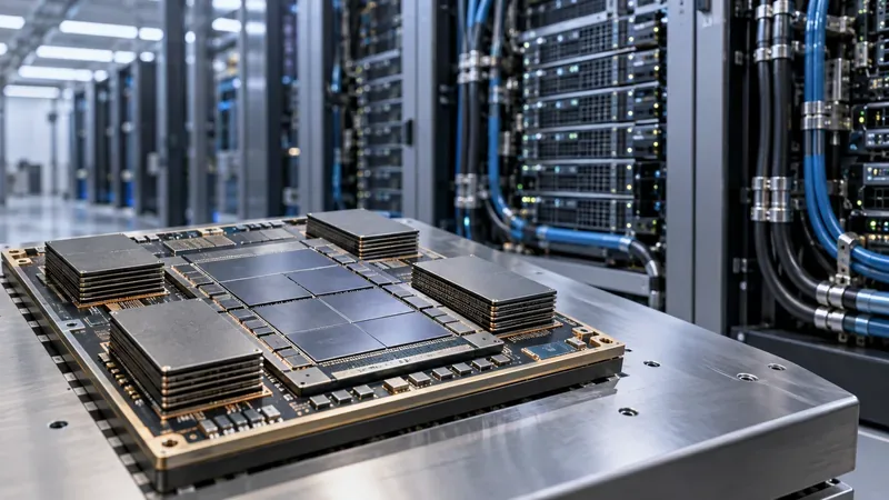
TSMC’s CoWoS family is central to many AI and HPC designs because it brings logic and HBM together on very large interposer-based systems. At its 2026 North America Technology Symposium, TSMC said it was producing 5.5-reticle-size CoWoS and planned a 14-reticle-size version for 2028 that could integrate roughly 10 large compute dies and 20 HBM stacks. The same roadmap includes SoIC 3D stacking and co-packaged optics. See TSMC’s 2026 technology symposium announcement.
The significance is architectural. As package area expands, designers can scale compute and memory without forcing every function onto one monolithic die. But larger packages make warpage, thermal gradients, substrate quality, interconnect integrity, power delivery, test strategy, and assembly yield harder to control.
Intel is betting on bridges plus vertical stacking
Intel’s packaging portfolio approaches the same problem with a different set of building blocks. EMIB embeds small silicon bridges in the substrate to connect dies laterally, while Foveros technologies support vertical stacking. Intel said in July 2026 that its New Mexico facilities were scaling packages beyond eight times the conventional reticle area, with plans to go beyond 12 times by 2028. Its latest EMIB-T adds through-silicon vias to improve power delivery and routing for demanding HBM-based systems. See Intel’s 2026 advanced-packaging overview.
This illustrates why packaging technologies should not be compared by a single metric. A full silicon interposer, an embedded silicon bridge, an RDL interposer, and a hybrid-bonded 3D stack make different trade-offs in bandwidth, cost, package area, thermal behavior, and manufacturing complexity.
Samsung is combining 2.5D, 3D, and memory integration
Samsung offers silicon-interposer and bridge-based 2.5D packaging as well as 3D stacking. Its current advanced heterogeneous integration material describes 3D Cube-T using TSV and thermal-compression bonding and 3D Cube-H under development with bumpless hybrid copper bonding. Samsung also continues to position I-Cube and X-Cube as part of its broader foundry-plus-memory strategy. See Samsung’s advanced heterogeneous integration overview.
The unresolved question is not whether these techniques are technically useful. It is which combinations can be manufactured at high yield, at the required package size, with the necessary HBM supply, and at a cost customers will accept.
Geography is becoming a manufacturing specification
The race is also about where each production stage happens. The most resilient supply chain is not necessarily the one with the most fabs; it is the one that can connect wafer fabrication, packaging, substrates, memory, test, equipment, materials, and engineering talent with manageable cycle time and risk.
Region
Current verified direction
Why it matters
Taiwan
TSMC continues major N2 and advanced-packaging investment and remains the center of its most mature leading-edge manufacturing ecosystem.
Dense supplier networks, accumulated process learning, and close coupling of front-end and packaging remain difficult to reproduce quickly.
United States
Intel is producing 18A domestically; TSMC’s Arizona plan has expanded to six logic fabs, two advanced-packaging facilities and an R&D center; Amkor is building a large advanced packaging/test campus in Arizona.
The U.S. is trying to close the gap between domestic leading-edge wafers and domestic high-volume advanced assembly.
South Korea
Samsung is advancing 2nm logic, HBM, and 2.5D/3D integration while Korea is also funding advanced-packaging infrastructure programs.
Co-location of memory, logic, and packaging can be strategically valuable for AI systems.
Japan
Rapidus is developing 2nm logic and a linked chiplet/advanced-packaging R&D flow, targeting mass production in 2027.
Japan is attempting to restore domestic leading-edge logic while leveraging deep strengths in materials and equipment.
Europe
EU Chips Act pilot lines such as NanoIC and FAMES are expanding access to advanced process R&D and pre-industrial-scale experimentation.
Europe is strengthening technology development and prototyping, although pilot-line capability should not be confused with large commercial AI-chip production capacity.
TSMC’s current Arizona page says its U.S. investment plan has grown to $265 billion and includes six logic fabs, two advanced-packaging facilities, and an R&D center, with the first advanced-packaging fab entering initial construction stages in early 2026. See TSMC Arizona’s current project summary.
Advanced packaging is also becoming a U.S. industrial-policy priority in its own right. Amkor broke ground in 2025 on an Arizona packaging and test campus whose planned investment was expanded to $7 billion, with production expected to begin in 2028. In June 2026, TSMC and Amkor announced a 10-year agreement for advanced packaging and testing collaboration in Arizona. See the TSMC-Amkor partnership announcement.
At the R&D level, the U.S. Department of Commerce announced in July 2026 letters of intent totaling $874 million for compute-supply-chain research that includes advanced packaging, substrates, materials, photonics, architectures, and memory. See the NIST announcement.
Europe is taking a different route. The EU opened the NanoIC pilot line at imec in February 2026, a €2.5 billion program with €700 million in EU funding, focused on next-generation semiconductor technology beyond 2nm at near-industrial R&D scale. FAMES at CEA-Leti, inaugurated in January 2026, focuses on ultra-low-power technologies. These facilities strengthen research access and process development, but they are not equivalent to announcing a new high-volume foundry. See the European Commission’s NanoIC announcement.
China is also pursuing domestic semiconductor manufacturing and packaging capability. In 2026, Chinese national policy continued tax support for qualifying semiconductor production and advanced packaging/test companies, while a national 2.5D chiplet-interconnect standard took effect on March 1, 2026. Those measures show continued ecosystem development, but they do not by themselves establish the production status or competitiveness of any particular leading-edge process. See the 2026 NDRC tax-policy notice and the national 2.5D chiplet-interface standard.
The hardest bottlenecks are moving into the interfaces
The next stage of competition will be decided less by isolated component specifications and more by interfaces between components and manufacturing stages.
Logic-to-memory bandwidth: More HBM stacks are useful only if routing, signal integrity, package area, and power delivery scale with them.
Thermals: Stacking dies shortens electrical paths but can make heat removal harder. Cooling becomes a package-design issue, not just a server-rack issue.
Known-good-die testing: A complex package can contain many expensive dies. Testing before assembly becomes critical because one defective component can destroy the value of the full package.
Substrates and interposers: The most advanced logic wafer is not useful if a package cannot be built at the required dimensions, routing density, flatness, and volume.
Hybrid bonding: Direct copper-to-copper bonding can increase interconnect density and reduce connection length, but manufacturing cleanliness, alignment, yield, and thermal stress become tougher.
Co-packaged optics: Moving optical I/O closer to compute can reduce the energy and latency of moving data, but it adds another manufacturing discipline to an already complex package.
This is why the semiconductor race increasingly rewards companies that can co-design transistors, chiplets, memory interfaces, package structures, test flows, power delivery, and cooling. The “back end” is no longer a low-value finishing step. For advanced AI systems, it is part of the architecture.
What to watch next
The easiest mistake is to treat every roadmap announcement as equivalent. It is more useful to rank evidence from easiest to hardest: technology demonstrations first, then risk production, customer tape-outs, production qualification, high-volume manufacturing, and finally sustained yields and shipment economics.
For fabrication, watch whether TSMC’s N2 family continues to ramp, whether Intel can broaden external adoption of 18A-family processes, whether Samsung converts 2nm engagements into durable volume, and whether Rapidus can move from pilot-line success to commercial-scale production in 2027.
For packaging, watch package size, HBM count, hybrid-bond pitch, substrate strategy, test methodology, thermal limits, and actual capacity. TSMC’s expansion of CoWoS, Intel’s larger EMIB/Foveros systems, Samsung’s hybrid-bonding work, and Rapidus’ panel-scale RDL experiments all point in the same direction: the package itself is getting larger, denser, and more system-like.
Geographically, watch whether new U.S., Japanese, Korean, and European investments create self-sustaining supplier clusters rather than isolated flagship facilities. A fab without nearby packaging, materials, spare parts, test, skilled labor, and customer engineering support can still face long cycle times and hidden dependencies.
How to check whether a chip-race claim is meaningful
Before accepting a headline about a new “leading” chip technology, run a quick reality check:
Is the claim about a prototype, risk production, or high-volume manufacturing?
Does the source state an actual production date, or only a target?
Is the node label being compared as if “2nm” meant the same thing across foundries? It does not.
Does the announcement cover wafer fabrication only, or also packaging, memory integration, and test?
Are package dimensions, HBM integration, yield, power delivery, and thermals discussed, or only transistor density?
Is the new facility a commercial-volume fab, an R&D pilot line, or a packaging/test site?
Are investment figures committed, under construction, or still conditional on incentives and future demand?
If an announcement passes those checks, it is more likely to represent a meaningful shift in semiconductor capability rather than a roadmap milestone presented without manufacturing context.
The race is no longer won on the wafer alone
The global semiconductor contest is still about who can make the most advanced transistors, but that is no longer enough. AI has made memory bandwidth, interconnect density, package size, test, thermals, and supply-chain geography inseparable from compute performance.
Taiwan remains the center of the most mature leading-edge foundry and advanced-packaging ecosystem. The United States is rebuilding front-end and advanced-packaging capacity at an unprecedented scale. South Korea is combining memory, logic, and packaging strengths. Japan is trying to return to leading-edge logic while building a connected chiplet ecosystem. Europe is expanding shared R&D infrastructure, and China continues to strengthen domestic manufacturing and packaging policy support.
The most important competition, therefore, is not simply “2nm versus 2nm.” It is the race to deliver a complete, manufacturable system: leading-edge logic, memory, package, power, cooling, testing, yield, and volume—together.