Home
» Technology
»
Next-Gen Semiconductors: How AI and Supercomputing Are Moving Beyond Smaller Transistors
Next-Gen Semiconductors: How AI and Supercomputing Are Moving Beyond Smaller Transistors
The short answer: AI gains now come from the whole semiconductor system
The next generation of AI and supercomputing hardware is not being powered by one breakthrough. It is being built from several technologies that have to work together: gate-all-around transistors, backside power delivery, chiplet architectures, advanced packaging, high-bandwidth memory, faster die-to-die links, and increasingly optical networking. The practical result is more compute, more memory bandwidth, and better scaling without relying only on smaller transistor dimensions.
That matters because modern AI accelerators and scientific supercomputers often run into data-movement and power limits before they run out of raw arithmetic capability. A faster matrix engine helps only if model weights, activations, and intermediate results can reach it quickly enough. Likewise, adding more accelerators helps only if the package, rack network, memory system, cooling system, and software stack can keep them busy.
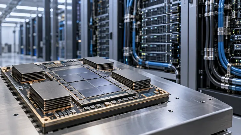
A multi-chip accelerator module with several stacked memory packages illustrates the direction of modern AI hardware: compute, memory, packaging, power delivery, and cooling are increasingly designed as one system.
1. New transistor structures improve efficiency, but they are only the starting point
Leading-edge logic is moving beyond the FinFET structure that dominated advanced chips for years. Gate-all-around, or GAA, designs wrap the gate around a nanosheet or similar channel structure, giving chip designers tighter electrostatic control as features shrink. This can improve performance, reduce leakage, or provide a better balance between the two.
TSMC says its 2-nanometer N2 process entered volume production in the fourth quarter of 2025, while its A16 technology combines nanosheet transistors with a backside power rail aimed particularly at high-performance computing products with dense power-delivery needs. TSMC has said A16 volume production is scheduled for the second half of 2026. See the foundry's A16 technology page and 2025 annual report.
Intel is following a related direction with Intel 18A. Its process combines RibbonFET GAA transistors with PowerVia backside power delivery. Intel reports that 18A entered production in 2025, while the enhanced 18A-P version entered risk production in June 2026. Intel also publishes comparative performance, power, and density claims for the node; those figures are vendor-reported and should be validated against a specific design rather than treated as universal chip-level gains. The current details are on Intel's 18A process page.
Backside power is important because advanced chips have to route both signals and power through extremely dense wiring. Moving part of the power-delivery network to the back side can free routing resources on the signal side and improve voltage delivery. For AI accelerators, where large arrays of compute units switch at high rates, that can be as important as transistor density.
2. Chiplets and advanced packaging are turning a package into a small computing system
Monolithic dies become harder and more expensive to scale as they grow. Chiplets offer another path: separate functions can be manufactured on process technologies that fit them best, then connected inside one package. A compute die may need the most advanced logic process, while I/O, cache, analog circuitry, or other functions may not.
Packaging is what makes this practical. TSMC's CoWoS advanced packaging platform, for example, is designed to integrate multiple logic devices and stacks of high-bandwidth memory in a 2.5D package. TSMC specifically positions CoWoS for AI and HPC products, where short, wide connections between compute and HBM are critical.
Standards are also emerging to make chiplets less proprietary. The UCIe 3.0 specification, released in August 2025, supports 48 GT/s and 64 GT/s data rates and adds features for power efficiency, manageability, and more flexible multi-chip systems. UCIe does not make chiplets interchangeable overnight, but it gives the industry a common electrical and protocol framework for on-package links.
This approach is especially attractive when a company wants to build several accelerator variants from reusable building blocks. It is less attractive when package cost, thermal density, or design complexity outweighs the modularity benefit. A smaller product with modest memory and I/O needs may still be better served by a simpler monolithic device.
3. High-bandwidth memory is becoming as strategic as the accelerator itself
AI workloads repeatedly move large tensors between memory and compute units. That makes memory bandwidth a first-order design constraint. High-bandwidth memory, or HBM, addresses the problem by stacking DRAM dies and placing them physically close to the accelerator through a very wide interface.
HBM4 is now moving from roadmap language into commercial systems. Samsung announced commercial HBM4 shipments in February 2026 and said its product entered mass production with a sustained 11.7 Gb/s transfer rate, with capability up to 13 Gb/s. In May 2026, Samsung also announced shipment of HBM4E samples. Those details are available in Samsung's HBM4 production announcement.
SK hynix said in its second-quarter 2026 results that it began mass shipments of HBM4 during the quarter and planned to ramp production in the second half of the year. The company has also shipped 12-layer HBM4E samples. See the SK hynix Q2 2026 results for the current status.
Why does this matter in practice? NVIDIA's current Vera Rubin specifications list 288 GB of HBM4 on one Rubin GPU and 19.2 TB/s of GPU memory bandwidth. By comparison, AMD's MI350-series accelerators use HBM3E; AMD lists up to 288 GB and 8 TB/s for the MI355X. These are different architectures and should not be compared from one bandwidth figure alone, but both illustrate how memory capacity and bandwidth are now core accelerator specifications rather than secondary details. See the official NVIDIA Vera Rubin NVL72 specifications and AMD Instinct MI350 Series page.
4. Scale-up and scale-out interconnects determine whether many accelerators act like one
Large models and scientific simulations rarely fit neatly on one device. The system has to divide work across multiple accelerators and exchange partial results frequently. If communication is slow, expensive compute units sit idle.
That is why proprietary scale-up fabrics are advancing alongside the GPUs themselves. NVIDIA's Rubin platform uses sixth-generation NVLink; NVIDIA lists 3 TB/s of NVLink bandwidth per Rubin GPU and 216 TB/s across an NVL72 system. AMD uses Infinity Fabric across its accelerator platforms. For buyers, the important question is not just peak link bandwidth but how the fabric behaves under the exact collective operations, model-parallel patterns, and topology used by the application.
At the system-memory level, Compute Express Link is evolving as well. The CXL Consortium says CXL 4.0 doubles signaling speed from 64 GT/s to 128 GT/s, adds bundled ports, and expands memory reliability features. CXL is relevant when architects want coherent memory expansion, pooling, or disaggregation without treating every memory tier as a remote storage device.
5. Silicon photonics is moving closer to the switching silicon
Copper remains excellent for short, dense electrical connections, but optical links become increasingly attractive as distance and aggregate bandwidth rise. A major next step is co-packaged optics, where optical components are moved closer to the networking ASIC instead of living entirely in pluggable transceivers at the edge of a switch.
NVIDIA says its Spectrum-X Ethernet Photonics platform uses co-packaged optics and reports up to 5 times better network power efficiency than traditional pluggable-transceiver designs. That is a vendor comparison, not a guarantee for every data center topology, but it highlights the direction of travel: network power is becoming material enough that optical integration is now part of semiconductor system design. See NVIDIA's silicon photonics overview.
What this means for real AI and supercomputing workloads
Workload
Semiconductor features to prioritize
Why they matter
Large-model pretraining
HBM capacity and bandwidth, fast scale-up links, dense packaging, strong cooling
Training spends heavily on tensor movement and synchronized communication across many accelerators.
Long-context and agentic inference
Large HBM pools, efficient low-precision compute, high interconnect bandwidth, memory tiering
KV cache and repeated reasoning steps can make memory capacity and data movement more limiting than peak FLOPS.
Simulation codes often depend on double precision and sustained bandwidth rather than only low-precision tensor throughput.
Enterprise inference
Performance per watt, software compatibility, right-sized memory, PCIe deployment options
The best system may be one that fits existing servers and power envelopes rather than the highest-density rack architecture.
Custom accelerators
Chiplet strategy, packaging ecosystem, UCIe support, process maturity
Modularity can shorten reuse cycles, but packaging complexity and supply-chain qualification can offset the benefit.
A concrete example: why a faster GPU is not enough
Consider a team serving a large language model with long context windows. Suppose profiling shows that GPUs are frequently waiting on memory transfers and cross-GPU communication. Moving to a newer accelerator could help, but only if the new system also provides enough HBM capacity, faster memory bandwidth, and a topology that reduces communication stalls. Buying a device with more theoretical tensor performance while keeping the same memory and networking bottlenecks may deliver much less improvement than the headline specification suggests.
The same principle appears in traditional supercomputing. Oak Ridge National Laboratory's Frontier system combines AMD MI250X accelerators with HBM and a high-speed system interconnect. The Frontier user guide documents how compute, HBM, CPU-GPU links, and the Slingshot network work together. The hardware generation is older than 2026's newest AI platforms, but the architectural lesson is still current: sustained application performance depends on the path between compute, memory, and other nodes.
When is next-generation semiconductor hardware worth the upgrade?
An upgrade is most defensible when it solves a measured bottleneck rather than simply replacing an older part number. Before committing to a new accelerator generation, check the following:
Memory pressure: Does the model or simulation spill to host memory, require aggressive checkpointing, or force an inconvenient degree of model partitioning?
Bandwidth pressure: Are kernels memory-bound in profiling, or are accelerators spending meaningful time waiting for all-reduce and other collective operations?
Power and cooling: Can the rack, facility, and cooling loop support the new power density? Higher performance can still be a poor fit if infrastructure upgrades dominate cost.
Software readiness: Are the compiler, libraries, kernels, orchestration stack, and monitoring tools mature for the new architecture?
Precision requirements: Can the workload safely use lower-precision formats, or does it require FP64 or another higher-precision path?
Utilization: Will the workload keep the new hardware busy enough to justify its cost? Capacity that sits idle does not become economical because the chip is newer.
The tradeoffs are becoming more physical
Semiconductor progress is producing impressive capability, but the limiting factors are increasingly tangible. Advanced packages are larger and more difficult to manufacture. HBM stacks concentrate heat near high-power logic. Rack-scale systems can demand liquid cooling, dense power distribution, and specialized networking. Co-packaged optics can reduce networking power, yet introduces new manufacturing and serviceability considerations. Chiplets can improve modularity, but add validation, packaging, and yield-management work.
There is also a software tradeoff. Low-precision arithmetic such as FP8, FP6, or FP4 can greatly increase AI throughput, but software has to preserve model quality. Scientific codes may not be able to use the same shortcuts. A semiconductor feature is valuable only when the application stack can exploit it without violating accuracy or reliability requirements.
What to watch next
For the rest of 2026 and into 2027, the most useful signals are not just new node names. Watch whether TSMC's A16 and Intel's 18A-family processes move into broad customer products; how quickly HBM4 and HBM4E become available at scale; whether UCIe 3.0 creates meaningful multi-vendor chiplet interoperability; where CXL 4.0 appears in production systems; and whether co-packaged optics proves economical and serviceable at large deployment scale.
Those milestones will show whether the semiconductor industry can continue scaling AI and supercomputing without letting memory movement, power delivery, networking, and cooling consume the gains made by denser logic.
Bottom line
The future of AI and supercomputing is being powered less by a single “next node” and more by coordinated semiconductor engineering. GAA transistors and backside power improve the logic foundation. Chiplets and advanced packaging let designers assemble larger systems than a single die can comfortably provide. HBM4 feeds accelerators at extreme bandwidth. UCIe, CXL, NVLink, Infinity Fabric, and optical networking move data across progressively larger domains.
If you are choosing hardware, start with your workload's real bottleneck. For memory-bound AI, prioritize HBM capacity and bandwidth. For distributed training, prioritize the scale-up and scale-out fabric. For scientific computing, verify FP64 and library performance. For enterprise deployment, include power, cooling, software support, and integration effort in the decision. The fastest semiconductor on paper is not automatically the fastest or most economical system for your workload.