Home
» Technology
»
How Silicon Innovation Is Driving the Next Industrial Revolution: A Beginner’s Roadmap
How Silicon Innovation Is Driving the Next Industrial Revolution: A Beginner’s Roadmap
Industrial technology is entering a phase in which the most important advances are no longer coming from one kind of chip or one manufacturing breakthrough. They are coming from a stack of changes: denser logic, specialized accelerators, faster memory, chiplets, advanced packaging, new interconnect standards, and power devices made from materials such as silicon carbide.
That shift is visible in current policy and R&D activity. On September 8, 2026, the U.S. Department of Commerce finalized a CHIPS R&D award of up to $375 million with GlobalFoundries that includes work on advanced packaging and heterogeneous integration alongside quantum-related semiconductor technologies. Earlier, on July 29, 2026, Commerce announced letters of intent totaling $874 million for semiconductor R&D across integrated photonics, compute architectures, advanced packaging, substrates, materials, and memory. Those announcements do not guarantee that every technology will reach commercial scale, but they illustrate where the industry sees major bottlenecks and opportunities today. See the official GlobalFoundries award announcement and the $874 million compute-supply-chain R&D announcement.
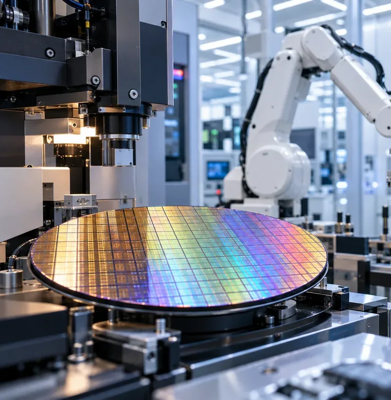
A silicon wafer sits on precision semiconductor equipment beside an automated robotic arm, illustrating how semiconductor manufacturing and industrial automation increasingly intersect.
Start With the Big Idea: “Silicon Innovation” Is Bigger Than Smaller Transistors
A semiconductor is a material whose electrical behavior can be controlled so it can switch, amplify, sense, store, or convert electrical signals. Silicon remains the dominant material for most digital logic, which is why people often use “silicon” as shorthand for the chip industry. But the next industrial wave depends on more than shrinking silicon transistors.
For decades, progress was often explained through the process node, a manufacturing generation associated with increasingly dense and capable transistors. Smaller nodes still matter, especially for high-performance computing. Yet many industrial systems are now improving through system-level choices: combining several dies in one package, moving data more efficiently, using application-specific accelerators, and selecting better materials for power conversion.
This distinction matters for a newcomer because “newer node” does not automatically mean “better industrial solution.” A motor controller, vision system, factory gateway, robot, or power converter may care more about determinism, reliability, temperature range, memory bandwidth, I/O, long product life, or energy efficiency than about having the smallest available transistors.
Build a Simple Mental Model Before Evaluating Products
It helps to understand five building blocks. You do not need to become a chip designer, but you should know what each layer contributes.
Concept
Plain-English meaning
Why it matters to industry
Chiplet
A smaller functional die designed to work with other dies inside one package.
Lets designers mix logic, memory, I/O, and specialized functions instead of building one enormous monolithic chip.
Advanced packaging
Techniques for placing and interconnecting multiple dies very closely in 2D, 2.5D, or 3D arrangements.
Can improve bandwidth, latency, power efficiency, and system density, but adds thermal, test, and manufacturing complexity.
Heterogeneous integration
Combining dies made with different process technologies or serving different functions.
Allows mature-node analog or I/O blocks to coexist with advanced logic, memory, photonics, or accelerators.
Accelerator
Hardware optimized for a specific workload, such as AI inference, vision, signal processing, or cryptography.
Can deliver better performance per watt than relying on a general-purpose CPU for every task.
Wide-bandgap power semiconductor
A power device built with materials such as silicon carbide (SiC) that tolerate higher electric fields and temperatures than conventional silicon devices.
Useful for efficient high-voltage power conversion in drives, charging, energy systems, and electrified machinery.
The U.S. National Institute of Standards and Technology describes advanced packaging as tightly assembling multiple chips with diverse functions so they can achieve performance and power improvements beyond conventional board-level packaging. Its National Advanced Packaging Manufacturing Program also highlights the hard parts: power delivery, heat removal, testing, repair, and reliability.
Understand Why Chiplets and Packaging Are Becoming Strategic
A monolithic die places most of a system’s functions on one piece of semiconductor material. That approach can be elegant, but very large dies become harder and more expensive to manufacture at high yield. Chiplets offer another path: partition a system into smaller dies and connect them with extremely short, high-speed links inside one package.
The key is not simply cutting a chip into pieces. The package must make those pieces behave like a coherent system. That requires dense interconnects, predictable latency, reliable power delivery, thermal management, and strong test coverage.
Open standards are becoming part of that story. The Universal Chiplet Interconnect Express, or UCIe, defines a package-level die-to-die interconnect. The official UCIe specifications page lists UCIe 3.0 as supporting 48 and 64 GT/s data rates, along with manageability and other improvements for scalable multi-chip systems. Standards do not guarantee that arbitrary chiplets can be mixed without engineering work, but they can reduce fragmentation and make interoperability a clearer design target.
Foundries are also treating packaging as part of system architecture rather than a final protective shell. TSMC, for example, describes its 3DFabric platform as a family of 3D stacking and advanced packaging technologies designed to integrate logic, memory, and specialty chips. Intel Foundry similarly positions advanced chiplet packaging as a way to build systems from multiple dies and interconnect technologies.
See Where the Industrial Impact Actually Appears
1. Smarter Machines at the Edge
Edge computing means processing data close to the machine, sensor, camera, or production line instead of sending every raw signal to a distant cloud. Better silicon makes it practical to place more compute near the physical process.
That can support machine vision, anomaly detection, robot perception, local control, and condition monitoring. The benefit is not merely “more AI.” Local compute can reduce communication delay, lower bandwidth demand, and keep some operations running even when cloud connectivity is limited. For industrial use, however, an AI accelerator must still coexist with real-time control, safety logic, networking, and deterministic timing requirements.
2. More Efficient Electrification
Factories consume large amounts of electricity through motors, drives, pumps, compressors, furnaces, HVAC, and power-conversion equipment. This is where silicon carbide (SiC) matters. SiC is not ordinary silicon; it is a wide-bandgap semiconductor material used especially in high-voltage power electronics.
The U.S. Department of Energy notes that SiC devices are suited to high-voltage applications and can improve efficiency in power-electronic systems. Its SK Siltron project summary explains that SiC wafers are important for power devices used in applications such as inverters, onboard chargers, and DC-to-DC conversion. Industrial equipment can benefit from the same general characteristics, although the economic case depends on voltage, switching frequency, thermal design, duty cycle, and component cost.
3. Faster Industrial AI and Simulation
Training large AI models usually happens in data centers, but industrial companies increasingly use accelerated computing for simulation, computer-aided engineering, digital twins, optimization, materials research, and production analytics. These workloads are strongly affected by memory bandwidth and how quickly processors exchange data.
That is why advanced packaging and high-bandwidth memory have become central to modern accelerators. Bringing memory and compute closer together can reduce the energy and time spent moving data. In practice, this means future industrial computing performance will depend as much on the package and memory system as on the arithmetic units themselves.
4. More Capable Sensors and Communications
Industrial systems also rely on analog chips, radio-frequency components, networking devices, timing chips, sensors, and photonics. Integrated photonics uses chip-scale optical components to move or process information with light. It is receiving attention because electrical interconnects face growing challenges as bandwidth requirements increase.
For a factory architect, the implication is simple: the next generation of industrial compute platforms will often be collections of specialized technologies rather than one universal processor.
Prepare Before You Choose Any Silicon Platform
A beginner can avoid expensive mistakes by defining the workload before comparing chips. Start with the physical system and work backward.
Define latency: How quickly must the system respond? A safety loop and a maintenance dashboard have very different timing requirements.
Measure data flow: How many cameras, sensors, motors, or network links are involved? What is the raw and processed data rate?
Estimate compute: Separate general CPU work from AI inference, signal processing, graphics, encryption, and real-time control.
Set the power budget: A fanless edge box, robot controller, and rack server live in different thermal envelopes.
Define environmental limits: Temperature, vibration, dust, electromagnetic noise, and expected service life can eliminate otherwise attractive parts.
Map lifecycle requirements: Industrial products may remain deployed far longer than consumer electronics. Availability, support, firmware maintenance, and qualification matter.
Then Match the Workload to the Right Silicon Strategy
Once the requirements are explicit, compare architectures rather than marketing labels.
For a machine-vision station, the right answer might be a CPU plus a modest AI accelerator and fast camera interfaces. For a mobile robot, performance per watt and integrated safety features may dominate. For a data-center digital-twin workload, high-end accelerators, high-bandwidth memory, and fast interconnects may matter most. For a motor drive, switching losses, voltage rating, thermal behavior, and power-module design can be more important than digital compute density.
This is also where chiplets should be evaluated realistically. They can improve modularity and allow different functions to use different process technologies, but they do not remove system engineering. Package cost, thermal density, yield across multiple dies, test strategy, interconnect reliability, and supply coordination all remain important.
Move From Evaluation to a Controlled Pilot
Do not begin by replacing an entire industrial platform. Choose one workload whose success can be measured clearly.
Create a baseline. Record current latency, throughput, energy use, failure rate, operating temperature, and maintenance burden.
Prototype with production-like data. Laboratory demos are useful, but industrial workloads often contain noise, timing variation, unusual edge cases, and sustained thermal load.
Test the whole system. Benchmark memory, storage, networking, I/O, thermals, power delivery, software, and recovery behavior—not only the processor.
Run long-duration tests. A platform that looks fast for five minutes may throttle, leak memory, accumulate errors, or behave differently after days of operation.
Validate supply and support. Confirm product lifecycle, second-source options where practical, security-update expectations, and qualification requirements before committing at scale.
Avoid the Most Common Beginner Mistakes
Buying the Biggest Benchmark Number
Peak TOPS, FLOPS, core count, or clock speed can be useful, but industrial performance depends on the actual workload. Memory bandwidth, data movement, software support, precision format, real-time behavior, and thermal limits can dominate.
Chiplets can improve reuse and yield economics in some designs, but packaging, interposers, testing, substrates, and thermal solutions can be expensive. The business case must be evaluated at the system level.
Ignoring Heat and Power Delivery
Higher compute density puts more power into a smaller area. Advanced packaging makes thermal engineering even more important because several active dies may sit close together. Cooling and power-delivery limits should be part of architecture selection from the beginning.
Confusing Announced Investment With Available Capacity
Fab announcements, R&D awards, and planned production milestones are important signals, but they are not the same as qualified parts shipping in volume. Always distinguish a funding announcement from a commercial product schedule.
Treating “Silicon” as One Technology
Industrial electronics use a portfolio: leading-edge logic, mature-node microcontrollers, analog chips, sensors, memory, silicon carbide power devices, and sometimes photonics. The best architecture combines the right technologies instead of forcing every function onto the newest node.
What the Next Industrial Revolution Will Look Like
The most important change is not that every factory will suddenly become autonomous. It is that computing, sensing, communication, and power conversion are becoming more capable at the same time. Silicon innovation is pushing intelligence closer to machines, increasing the practical scale of industrial AI, enabling more efficient electrification, and giving system designers new ways to combine specialized hardware.
For newcomers, the safest way to engage with this shift is to stay workload-first. Learn the basic vocabulary, quantify the physical constraints, choose architecture based on the job, pilot with real data, and validate reliability and supply before scaling. The industrial winners are unlikely to be the companies that simply buy the newest chip. They will be the ones that understand where semiconductor innovation changes the economics or capability of a real process—and where it does not.